
How is a PCB manufactured?
The beginning step of any PCB manufacture is the design. Our express manufacturing services ensure that prototype requirements are manufactured and dispatched to meet all customer expectations.
Smart Electronics offers inexpensive PCBs for quantities as little as 1 piece to as high as thousands pieces in relatively short time. Our PCB designers as checking every design before starting production, which eliminates the most potential problems like short circuits, un-poured templates etc.
The steps of PCB manufacturing process as follows:
Specification
As a professional PCB manufacturer, we continue to invest in state-of-the-art automation equipment and keep updating PCB manufacturing process and technologies. Smart Electronics offers maximum 70 layers so ask us as many layers as you want. Click ‘Smart Data’ to see more options.

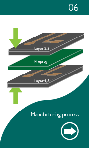
06 Bonding

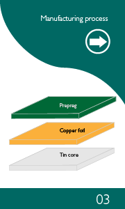
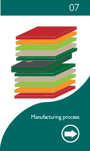
07 Lay-up, Lamination and Press
Press PCB inner cores, prepregs and copper foils together to multilayer PCB panels

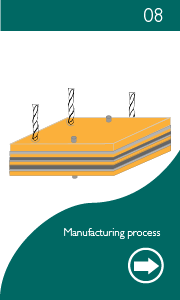
08 Drilling
Locate precisely onto CNC drill machine and drill all holes and plated slots.

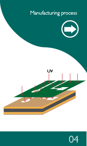
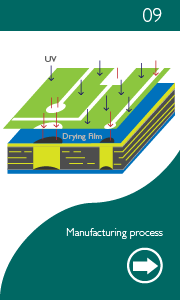
09 Imaging Outer Layers
Laminating the dry film and apply photoimageable plating resistand UV image tracks. Also Exposing circuitry and holes.

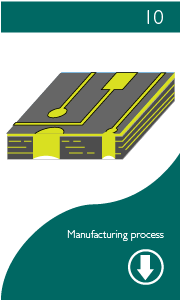
10 Electrolytic Plating
Exposed areas of panel are electrolytically plated. Dryfilm is stripped exposing unwanted copper. Unwanted copper is etched away and Tin is stripped.
Surface finish materials
*** We have multiple types of surface finish available according to customers’ specific demands
under the EU Reduction of Hazardous Substances (or “RoHS”) legislation
● Immersion Gold / ● HGSL(Lead Free) / ● Pre-Flux / ● Hard gold / ● Tin

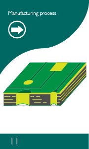
11 Solder resist mask printing
Soldermask is used to define the component holes and pads. Apply the photoimageable solder mask, expose, develop and final cure.

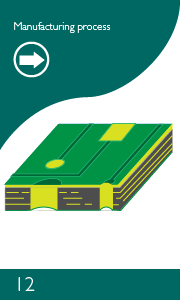
12 Surface finishing
The finish has two critical functions, to protect the exposed copper circuitry and to provide solderable surface when assembling (soldering) the components to printed circuit board.

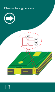
13 Fabrication
Panels are silk-screened prior to fabrication and profile individual circuits on V-cut or scoring machine.

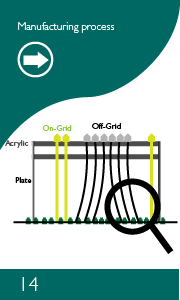
14 Bare board testing
Either bed of nails or flying probe. Using ICT, Smart Electronics can efficiently test individual components and their electronic characteristics

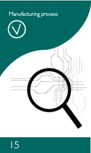
15 Final Inspection
Including outgoing inspection and reliability Test. Technical drawing and order specification compliance measurements also carried out at final inspection.
Automated Optical Inspection(AOI)
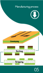
Automated Optical Inspection (AOI) equipment is inspect all inner PCB layers before proceeding the next step in PCB manufacturing. This process identifies opens, shorts, and reduced traces, after pcb etching. It is better to locates problems early in process, prior to lamination.